線上影音
Home > ANSYS Q3D 教學 > Basic Capacitive Touch Screen Panel Design with Q3D
本文介紹如何以Q3D2015.1模擬投射式電容觸控面板,並以直徑5mm銅柱模擬手指對Touch Screen Panel (TSP)互電容與自電容感應值的影響。另外,也對於模擬精度的設定,與模擬很薄導體(如ITO)的加速...等,做討論。The article is intended to introduce how to simulate projected capacitive touch-screen panel with Q3D2015.1 (R16.1), which is the best 3D EM solver (electromagnetic field solver) for RLC extraction. The ability to analyze any kind of 3D geometry (not only for layered structure) and consider fringe effect are the points.
-
Q&A
7.2 Can Q3D export S-parameter model?
7.3 How to decide the right "percent error" for accuracy of TSP? (important)
7.4 How to decide the right "solution order" for Q3D to speed up? (important)
7.5 What is the major difference between Q3D and other RLC extractor? (important)
7.6 What is the meaning of the diagonal entrys in C matrix, self-capacitor?
7.7 What is the minimized size that is recommended for sensitivity simulation?
7.8 Is there any special function of Q3D that is good for complex TSP design (as in-cell)?
7.9 How to estimate the linearity performance of TSP with a very simple delta-Cm result?
7.11 As we know, capacitor is frequency dependent, but is it voltage dependent? No
-
Reference
![]()
下圖所示為一雙層ITO電容 式觸控面板的sensor pattern正視圖
下圖則為其疊構的側視圖


2.1 Insert a new Q3D design
2.2 General setup
[Tools] \ [Options] \ [General Options],勾選[Insert a design of type],讓每次打開Q3D時,可以自動開啟一個2D/3D design
2.3 HPC setup (if you have HPC option, it will speed up your simulation time very much)
For different hardware resources and different distribution types, the HPC setting may be different.
2.4 Create cover glass, film and ITO pattern using [Draw box]
Substrate (film) thickness 100um、ITO thickness 1um (0.1u*10),Rx width 1mm,Tx width 4.9mm with gap=0.1mm,pitch=5mm,cover glass thickness 0.7mm
實際ITO層的厚度很薄(約0.1um),為了讓EM solver可以順利求解,本例中我們放大等效厚度為0.1u*10=1um. (導電率也要降低10倍)
2.5 Create a conductive finger using [Draw cylinder]
, and set it's radius as 2.5mm, height 3mm.
2.6 Re-assign ITO trace pitch、ITO thickness、film thickness、cover lens thickness、Tx\Rx width with different parameters, then you can simulate geometry sweeping later.
To check the parameters you have defined, just select the design in project window and find the content in the [Properties] window


-
Assign Material (add ITO material to material library)

ITO的面電阻一般為100~300W/o,視厚度與長在何種材質上而定,長在玻璃上的面阻值一般比長在film上的小。假設ITO厚度為0.1um,透過電阻率(resistivity, r)與導電率(conductivity, s)的換算,300W/o的ITO導電率為33333 (siemens/m)。換算方式如下所示:
這ITO材質需要user於軟體中自建:先選定要設材質為ITO的object,[Modeler] \ [Assign Material] \ [Add Material]
本例因為有將ITO厚度放大10倍(0.1u*10=1um)便於求解,故也要把導電率等效降低10倍(33333->3333 siemens/m)。如果不放大等效厚度而要硬解0.1um的真實厚度,軟體會提示如下的錯誤訊息:表示存在有極其微小的幾何結構,其小於目前選定刻度單位(mm)的1/1000,這會造成mesh resolution非常困難。
稍後我們會另外再介紹thin conductor技術,是另一種不用放大厚度可專解這種薄導體的技術 ,更快更好。


4.1 Auto identify nets
4.2 Assign sink\source
Assigning sink\source by net is necessary for RL solver. In case, you run CG solver only, this step can be ignored.


5.1 Analysis Setup
舊版的Q3D solution order分三檔:Normal, High, Very High
Q3D 2015.1(R16.1)起,solution order分四檔:Normal (default), High, Higher, Highest
Q3D 2016.x(R17.x)起,High by default for solution order
5.2 Validation check
5.3 Run Analysis


6.1 Convergence
It is quit obvious that the number of passes for the case with finger is more than the one without finger. Why?
The answer is about "mesh". Please see next step.
6.2 Plot Mesh
Plot mesh of finger and dielectric layer (film) between Tx and Rx ITO.
The one with finger requires much more number of mesh to converge less than percent error less 1% twice.
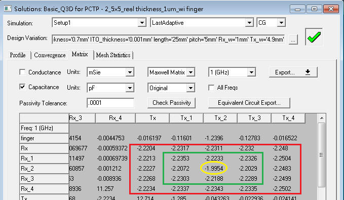
6.3 C Matrix
6.3.1 no finger touch
Check the mutual C elements circled by red line above, and except the outer elements including different fringe effects of boundary. All of the elements circled by green line "should be" the identical values. So, for this case, the significant figures of these elements are just 0.1pF. In case you want to get more accuracy for some applications as in-cell or fingerprint recognition, to set smaller "percent error" (0.1~0.05) and larger "max. number of pass" is advised.
以此例來說,當percent error取1%時,內圈的所有3x3單元,Cm相同值也只達pF小數點以下一位(2.21~2.26pF),也就是精度有效位元只達100fF,這其實是不夠的。 對於觸控的應用,因為5phi的手指引起的delta-Cm約150~200fF,所以模擬的精度最好能達到pF小數點以下兩位,也就是10fF才夠。我們可以藉此來評斷模擬的percent error設的夠不夠小。此題若直接把percent error從1%改成0.1%,還會遇到難以收斂的問題,所以這類題目最正確的做法是用thin conductor,且把percent percent設0.1%. refer to 7.8
6.3.2 with finger touch
Delat-mutual C = 2.25-1.99p = 260fF with 5phi touch size.
6.4 Export Touchstone or SPICE model


-
Q&A
7.1 Can Q3D plot E-field?
Ans:Q3D can plot Q or V field, and SI2D (2D solver in Q3D) can plot E-field for 2D cross section.
7.2 Can Q3D export S-parameter model?
Ans:Yes, as step 6.4 shows. The only one has to be noted is that the 1/10 lambda rule should be confirmed.
7.3 How to decide the right "percent error" for accuracy of TSP?
Ans:As step 6.3.1 explain, for the un-touch case, set a certain percent error as criteria to get the accuracy\precision enough, and that makes all of the mutual C elements in green line are as same as possible. In general, for the touch panel application, to set percent error as 0.1% with thin conductor is preferred, not 1%.
7.4 How to decide the right "solution order" for Q3D to speed up?
Ans:In general, set Solution Order as [Normal] by default is good (an001 3.3.1, an001 3.3.2), but for the cases hard to converge as an001 3.3.3, 6.1, 7.8, set Solution Order as [Higher\Highest] is better. High order的作用是透過較高階數的矩陣數值運算,以較少的mesh而可以較快達到所要求的percent error。所以high order會讓mesh時間減少,但matrix solver時間卻會增加。對於很難收斂的題目(for example, percent error£0.1),建議可設較高階的order。
7.5 What is the major difference between Q3D and other RLC extractor?
Ans:Q3D is not only the most accurate 3D EM solver for RLC extraction counting fringe effect, but also good to the application with very thin conductor layer as ITO.
For example, one pair of parallel copper plats with area A=1mm2, and the space between the plats is d=0.1mm FR4 (Er=4.4).
The "ideal" C that means without fringe effect should be C=e*A/d=Er*Eo*A/d=4.4*8.85e-12(F/m)*1e-6/1e-4=389.4fF
Let's surround the copper plat with a conductive ring (space 50um) to minimize the fringe effect around edges of the plate
為何圍繞於平行電極板外圍的導體距離更近的話(<50um),平行電極板夾出的電容會更小於389fF?
Why will the C value less than 389fF, if the space between copper plats and outer guard ring less than 50um?
於平行電極板外圍一圈導體(guard ring),可以框住外擴的電力線流梳(outer fringe),減少fringe的影響,但這一圈guard ring距離平行電極板最佳距離大約是0.5*極板距離,若距離太近反而平行電極板所夾出的電容會變小。因為電極板與guard ring金屬彼此會交互影響,導致單位面積可蓄積的感應電荷變少,即平行電極板所夾出的電容變小。
7.6 What is the meaning of the diagonal entrys in C matrix, self-capacitor?
Ans:大家都知道電容是兩面平行電極板間儲存的電荷,所以互電容是很直覺可以理解的,但什麼是自電容?
對於Maxwell Matrix,自電容是所有作用在此物件上的互電容總合,即導體本身在空間上對外看出去,所有其他的導體對其電力線牽引所形成的所有 感應電荷累積總合,也就是它與其他導體的所有互電容總和。基於電荷平和的基礎,如果不考慮無窮遠處的絕對參考地影響,那導體X的電容特性應該是Cx_self = SUM(all of Cx_mutual),這就是為何在Q3D的Reduce matrix內設[floating at infinity]後,C of Maxwell matrix的任一行或列總和近乎=0的原因
Please refer to another article in the website:self-capacitor and mutual-resistance
7.7 What is the minimized size that is recommended for sensitivity simulation?
Ans:As step 6.3.1 explain, a 5x5 array is suggested to be simulated, but only the 3x3 inner elements of the array are used. (模擬5x5, 但只使用其中的3x3)
7.8 Is there any special function of Q3D that is good for complex TSP design (as in-cell)?
Ans:Thin conductor technology, that is 2D sheet boundary to speed up RLC calculating. By the way, HPC (high performance computing) also speeds up significantly.
To re-do the 5x5 project with thin conductor and targeted percent error=0.1% twice
Normal order -- it takes 4:53:40, more mesh, and much slower
Highest order -- it takes 1:22:37, less mesh, and much faster
手指出現處(黃線圈起)的互容變化:Delat-mutual C = 2.208-1.969p = 239fF with 5phi touch size
Thin conductor can speed up 10x~ for touch-screen panel simulation, it is very impressive.
7.9 How to estimate the linearity performance of a TSP with a very simple delta-Cm result?
Ans:
abs
(pF) - abs
(pF) =
(fF)
在手指出現位置正中心點的互容變化是239fF,這表示的是sensitivity。 (以5 phi touch來說算是很好的了)
左右(by Tx)離手指5mm距離處的感應單元變化27~30fF,明顯比上下(by Rx)離手指5mm距離處的感應單元變化10fF來的大,這代表感應的靈敏度上下左右並沒有完全對稱,這會反映在手指從左上到右下(斜劃線)會出現ripple的軌跡。改進的方法是略為加大Rx的寬度即可。
增加Rx的寬度雖然可以改善線性度,但會增加手指未出現時的基礎互容(base Cm),,這又是另外一個需要trade-off問題,所以另外衍伸出Rx分支或挖洞的設計。請參閱本站另一篇TSP optimized design。
如果習知以上的基本觀念,其實要做觸控的線性度評估,並非一定要花時間跑連續很多個點
7.10 Why to set copper material for finger model? Is it different if assign other conductor to finger?
Ans:In mass production, a copper stick is normally used for finger testing. Any "conductor" with different conductivity will get exactly the same result of capacitor, no matter for self-capacitor or mutual-capacitor. In a word, the different conductivity of finger just affects the settling time, not the value of capacitor.
7.11 As we know, capacitor is frequency dependent, but is it voltage dependent?
Ans:The answer is No. C=eps*A/d, where eps. means relative permittivity, A means area, d means distance.
Based on this basic formula, it should be easy to understand capacitor is frequency dependent, but not voltage dependent. Unfortunately, there are still a lot of EE engineers of TSP field misunderstand this and think C is voltage dependent, due to their own "C measurement experience" form the sensing IC.
Please note that, I say it just happens on TSP IC sensing experience. Due to TSP IC sensing technology (not LCR meter), no matter using constant-voltage or constant-current charging method, is based on the charge Q that is charged\detected to calculate C (Q=C*V), it is very important to know that settling time of voltage level affects the C measurement result very much, and you have to make sure the sensing circuit (charge\discharge) works with enough time period to get right result.
如果你用不同的電壓設定,量出的電容值會變,那表示低電壓設定下所量出的電容值因為充電時間不足(non-settling),換算出的電容值是錯的,可以試著拉長充放電時間週期,就可以驗證這件事。


-
Reference
[1] 王俊凱, "以統計方法產生的觸控板感測器模型與最佳化", 交大碩士論文, 2009
[2] S Kim, W Choi,"A Highly Sensitive Capacitive Touch Sensor Integrated on a Thin-Film-Encapsulated Active-Matrix OLED for Ultrathin Displays", IEEE Trans. on Electron Devices, vol. 58, no. 10, Oct. 2011 (Samsung study OLED with Q3D)